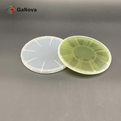
Oblea sic epitaxial
(42)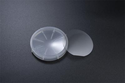
Dispositivo de potencia de 2 pulgadas Transistor de alta movilidad de electrones Wafer epitaxial
Precio: Negotiable
MOQ: 5
El tiempo de entrega: Negotiable
Marca: Ganova
Destacar:sic epitaxial wafer 2 Inch, Power Device sic epitaxial wafer, High Electron Mobility Transistor Epitaxial Wafer
Introduction to GaN on Silicon HEMT Epi wafer Silicon based gallium nitride HEMT epitaxial wafer is a high electron mobility transistor (HEMT) epitaxial wafer based on gallium nitride (GaN) material. Its structure mainly includes AlGaN barrier layer, GaN channel layer, AlN buffer layer, and silicon ... Ver más
➤ Visitar Sitio web
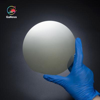
2 pulgadas GaN en la oblea de silicio HEMT Epi para el dispositivo de energía
Precio: Negotiable
MOQ: 5
El tiempo de entrega: Negotiable
Marca: Ganova
Destacar:GaN On Silicon HEMT Epi Wafer, 2 Inch Epi Wafer, Power Device Epi Wafer
Introduction to GaN on Silicon HEMT Epi wafer Silicon based gallium nitride HEMT epitaxial wafer is a high electron mobility transistor (HEMT) epitaxial wafer based on gallium nitride (GaN) material. Its structure mainly includes AlGaN barrier layer, GaN channel layer, AlN buffer layer, and silicon ... Ver más
➤ Visitar Sitio web
Barrera de AlGaN 4 pulgadas de GaN en la oblea de silicio HEMT Epi de nitruro de galio GaN-en-Si
Precio: Negotiable
MOQ: 5
El tiempo de entrega: Negotiable
Marca: Ganova
Destacar:4 inch sic epitaxial wafer, 4 inch sic epi wafer, 4 inch sic epi wafers
Introduction to GaN on Silicon HEMT Epi wafer Silicon based gallium nitride HEMT epitaxial wafer is a high electron mobility transistor (HEMT) epitaxial wafer based on gallium nitride (GaN) material. Its structure mainly includes AlGaN barrier layer, GaN channel layer, AlN buffer layer, and silicon ... Ver más
➤ Visitar Sitio web
6 pulgadas GaN en silicio HEMT Epi Wafer dispositivo de alimentación Nitruro de galio GaN en Si
Precio: Negotiable
MOQ: 5
El tiempo de entrega: Negotiable
Marca: Ganova
Destacar:6 Inch sic epitaxial wafer, 6 Inch sic epi wafer, 6 Inch sic epi wafers
Introduction to GaN on Silicon HEMT Epi wafer Silicon based gallium nitride HEMT epitaxial wafer is a high electron mobility transistor (HEMT) epitaxial wafer based on gallium nitride (GaN) material. Its structure mainly includes AlGaN barrier layer, GaN channel layer, AlN buffer layer, and silicon ... Ver más
➤ Visitar Sitio web
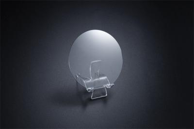
GaN láser violeta en el silicio 2 pulgadas GaN en el silicio HEMT Epi oblea UV LD Epi oblea
Precio: Negotiable
MOQ: 5
El tiempo de entrega: Negotiable
Marca: Ganova
Destacar:2 inch sic epitaxial wafer, 2 inch sic epi wafer, 2 inch sic epi wafers
Introduction to GaN on Silicon HEMT Epi wafer Silicon based gallium nitride HEMT epitaxial wafer is a high electron mobility transistor (HEMT) epitaxial wafer based on gallium nitride (GaN) material. Its structure mainly includes AlGaN barrier layer, GaN channel layer, AlN buffer layer, and silicon ... Ver más
➤ Visitar Sitio web
2 pulgadas de GaN en el silicio azul LD Epi oblea GaN láser azul en el silicio
Precio: Negotiable
MOQ: 5
El tiempo de entrega: Negotiable
Marca: Ganova
Destacar:2 inch sic epitaxial wafer, 2 inch sic epi wafer, 2 inch sic epi wafers
Introduction to GaN on Silicon HEMT Epi wafer Silicon based gallium nitride HEMT epitaxial wafer is a high electron mobility transistor (HEMT) epitaxial wafer based on gallium nitride (GaN) material. Its structure mainly includes AlGaN barrier layer, GaN channel layer, AlN buffer layer, and silicon ... Ver más
➤ Visitar Sitio web
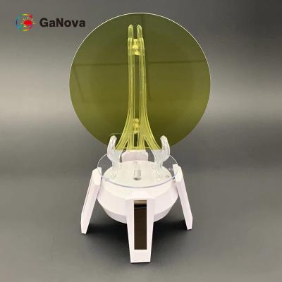
LED azul GaN en oblea de silicio Oblea epitaxial láser azul GaN
Precio: Negotiable
MOQ: 5
El tiempo de entrega: Negotiable
Marca: Ganova
Destacar:Silicon Based Gallium Nitride Epitaxial Wafer, HEMT epitaxial wafer, 4 inch sic epitaxial wafer
Introduction to GaN on Silicon HEMT Epi wafer Silicon based gallium nitride HEMT epitaxial wafer is a high electron mobility transistor (HEMT) epitaxial wafer based on gallium nitride (GaN) material. Its structure mainly includes AlGaN barrier layer, GaN channel layer, AlN buffer layer, and silicon ... Ver más
➤ Visitar Sitio web
2 pulgadas de GaN en el silicio verde LED Epi wafer Nitruro de galio en el silicio
Precio: Negotiable
MOQ: 5
El tiempo de entrega: Negotiable
Marca: Ganova
Destacar:2 inch sic epitaxial wafer, 2 inch sic epi wafer, 2 inch sic epi wafers
Introduction to GaN on Silicon Green LED Epi wafer GaN on Silicon Green LED Epi wafer are semiconductor structures formed on silicon substrate materials through epitaxial growth technology for manufacturing green light-emitting diodes (LEDs). It is a key intermediate material in the manufacturing of... Ver más
➤ Visitar Sitio web

4 pulgadas de GaN en el silicona verde LED Epi oblea SiC oblea epitaxial
Precio: 1000
MOQ: 5
El tiempo de entrega: Negotiable
Marca: Ganova
Destacar:4 inch sic epitaxial wafer, 4 inch sic epi wafer, 4 inch sic epi wafers
Introduction to GaN on Silicon Green LED Epi wafer GaN on Silicon Green LED Epi wafer are semiconductor structures formed on silicon substrate materials through epitaxial growth technology for manufacturing green light-emitting diodes (LEDs). It is a key intermediate material in the manufacturing of... Ver más
➤ Visitar Sitio web

4 pulgadas de UGaN en nitruro de galio sin dopaje de silicio en la oblea epitaxial de silicio
Precio: 1000
MOQ: 5
El tiempo de entrega: Negotiable
Marca: Ganova
Destacar:4 inch sic epitaxial wafer, 4 inch sic epi wafer, 4 inch sic epi wafers
Introduction to GaN on Silicon Green LED Epi wafer GaN on Silicon Green LED Epi wafer are semiconductor structures formed on silicon substrate materials through epitaxial growth technology for manufacturing green light-emitting diodes (LEDs). It is a key intermediate material in the manufacturing of... Ver más
➤ Visitar Sitio web

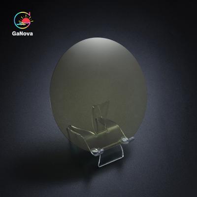
oblea sic epitaxial de 150.0m m +0mm/-0.2mm ningún plano secundario 3m m
Precio: Negotiable
MOQ: Negotiable
El tiempo de entrega: 3-4 week days
Marca: GaNova
Destacar:150.0 mm SiC Epitaxial Wafer, silicon carbide wafer 3mm, SiC Epitaxial Wafer No Secondary Flat
JDCD03-001-003 Overview SiC boules (crystals) are grown, machined into ingots, and then sliced into substrates, which are subsequently polished. A thin SiC epitaxial layer is then grown on top of this substrate to create an epi-wafer. Today, the semiconductor industry is expanding at a rapid rate, w... Ver más
➤ Visitar Sitio web
47,5 milímetros de ± oblea sic epitaxial 150,0 milímetro +0mm/-0.2mm to<11-20>±1° paralelo de 1,5 milímetros
Precio: Negotiable
MOQ: Negotiable
El tiempo de entrega: 3-4 week days
Marca: GaNova
Destacar:446mm SiC Epitaxial Wafer, 4 H epitaxial silicon wafer, UKAS SiC Epitaxial Wafer
47.5 mm ± 1.5 mm SiC Epitaxial Wafer 150.0 mm +0mm/-0.2mm Parallel to±1° JDCD03-001-003 Overview Currently, there are two main types of SiC wafers. The first type is the polished wafer, which is a single silicon carbide disc. It is made of high-purity SiC crystals, and can be 100mm or 150mm in diame... Ver más
➤ Visitar Sitio web

4H oblea sic epitaxial ≤0.2 /cm2 0.015Ω•cm-0.025Ω•cm 150,0 milímetro +0mm/-0.2mm
Precio: Negotiable
MOQ: Negotiable
El tiempo de entrega: 3-4 week days
Marca: GaNova
Destacar:4H SiC Epitaxial Wafer, silicon carbide wafer ISO9001, SiC Epitaxial Wafer 0.2 /Cm2
4H SiC Epitaxial Wafer ≤0.2 /Cm2 0.015Ω•Cm—0.025Ω•Cm 150.0 mm +0mm/-0.2mm JDCD03-001-004 Overview The 200-mm wafers can be used for a variety of applications. These wafers are 50% thinner than the standard silicon wafer, so the 200-mm diameter can be used for more SiC devices. The 200-mm size is muc... Ver más
➤ Visitar Sitio web

4H oblea sic epitaxial 0.015Ω•cm-0.025Ω•² 150,0 milímetro +0mm/-0.2mm del cm ≤4000/cm
Precio: Negotiable
MOQ: Negotiable
El tiempo de entrega: 3-4 week days
Marca: GaNova
Destacar:4H SiC Epitaxial Wafer, silicon epi wafer 0.025Ω•Cm, SiC Epitaxial Wafer 0.015Ω•Cm
4H SiC Epitaxial Wafer 0.015Ω•cm—0.025Ω•cm ≤4000/cm2 150.0 mm +0mm/-0.2mm JDCD03-001-003 Overview The next type is beta silicon carbide. Beta SiC is produced at temperatures higher than 1700 degrees Celsius. Alpha carbide is the most common, and has a hexagonal crystal structure similar to Wurtzite.... Ver más
➤ Visitar Sitio web

Sustrato de SiC de nivel P de 2 pulgadas para dispositivos de potencia y dispositivos de microondas
Precio: Negotiable
MOQ: Negotiable
El tiempo de entrega: 3-4 week days
Marca: GaNova
Destacar:P Level SiC Substrate, Microwave Devices silicon carbide substrate, 2 Inch SiC Substrate
P-Level 4H-N/SI260um±25um 2-Inch SiC Substrate For Power Devices And Microwave Devices JDCD03-001-001 2-inch SiC substrate P-level 4H-N/SI260μm±25μm for power devices and microwave devices Overview Key features Optimizes targeted performance and total cost of ownership for next generation power elec... Ver más
➤ Visitar Sitio web

Sustrato SiC de 2 pulgadas de 350 μm para electrónica de potencia exigente
Precio: Negotiable
MOQ: Negotiable
El tiempo de entrega: 3-4 week days
Marca: GaNova
Destacar:2 Inch SiC Substrate, Demanding Power Electronics 2 inch wafer, SiC Substrate 350um
P-Level 2-Inch SiC Substrate 4H-N/SI260μm±25μm For Demanding Power Electronics JDCD03-001-001 2-inch SiC substrate P-level 4H-N/SI260μm±25μm for power devices and microwave devices Overview High crystal quality for demanding power electronics As transportation, energy and industrial markets evolve, ... Ver más
➤ Visitar Sitio web
0.015Ω•cm-0.025Ω•CMP polaco óptico de la Si-cara de la C-cara sic epitaxial de la oblea del cm
Precio: Negotiable
MOQ: Negotiable
El tiempo de entrega: 3-4 week days
Marca: GaNova
Destacar:SiC Epitaxial Wafer C-Face, Optical Polish sic wafer, Si-Face CMP Sic Epitaxial Wafer
0.015Ω•cm—0.025Ω•cm SiC Epitaxial Wafer C-Face:Optical Polish,Si-Face CMP Overview A SiC wafer is a semiconductor material made of silicon. A silicon carbide wafer is a crystalline material that is made by etching the crystal. It is typically thin enough to be used for power semiconductor devices. T... Ver más
➤ Visitar Sitio web
nivel P del sustrato de carburo de silicio de 260 μm para dispositivos de potencia y dispositivos de microondas
Precio: Negotiable
MOQ: Negotiable
El tiempo de entrega: 3-4 week days
Marca: GaNova
Destacar:260um silicon carbide substrate, Power Devices Epitaxial Wafer, silicon carbide substrate P Level
4H-N/SI260μm±25μm 2-Inch SiC Substrate P-Level For Power Devices And Microwave Devices JDCD03-001-001 2-inch SiC substrate P-level 4H-N/SI260μm±25μm for power devices and microwave devices Overview We contribute to the SiC success story by developing and manufacturing market-leading quality SiC subs... Ver más
➤ Visitar Sitio web

Politipo Ninguno permitido SiC Epitaxial Wafer P-MOS P-SBD Grado D
Precio: Negotiable
MOQ: Negotiable
El tiempo de entrega: 3-4 week days
Marca: GaNova
Destacar:SiC Epitaxial Wafer P-MOS, D Grade silicon epi wafer, SiC Epitaxial Wafer P-SBD
JDCD03-001-004 Sic Epitaxial Wafer P-MOS P-SBD D Grade Polytype None Permitted JDCD03-001-004 Overview A SiC wafer is a semiconductor material that has excellent electrical and thermal properties. It is a high-performance semiconductor that is ideal for a wide variety of applications. In addition to... Ver más
➤ Visitar Sitio web