El FE dopó a GaN Substrates Resistivity > 10 el ⁶ Ω·Radioinstrumentos del cm
Precio: Negotiable
MOQ: Negotiable
El tiempo de entrega: 3-4 week days
Marca: GaNova
Destacar:ISO GaN Substrates, gan semiconductor wafer, Fe Doped GaN Substrates
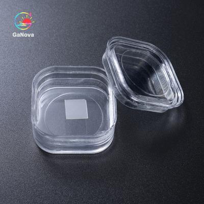
2inch C-face Fe-doped SI-type free-standing GaN single crystal substrate Resistivity > 106 Ω·cm RF devices The achieved breakdown voltage of the Fe-doped GaN epitaxial layer can be as high as 2457 V, which is attributed to the Fe-doped GaN epitaxial layer with higher resistance, which can sustain... Ver más
Contacta ahora
4 pulgadas 4H-SiC Substrato de nivel P SI 500.0±25.0μm MPD≤5/cm2 Resistividad≥1E5Ω·cm Para microondas de potencia
Precio: Negotiable
MOQ: Negotiable
El tiempo de entrega: 3-4 week days
Marca: GaNova
Destacar:Substrato de 4H-SiC de nivel P, Substrato de 4H-SiC para microondas, Substrato de 4 pulgadas de 4H-SiC
Nivel P SI los 500.0±25.0μm MPD≤5/cm2 Resistivity≥1E5Ω del substrato de JDCD03-002-002 4inch 4H-SiC·cm para los dispositivos del poder y de la microonda
Descripción
Sic se utiliza para la fabricación de dispositivos muy de alto voltaje y de alta potencia tales como diodos, transistores de... Ver más
Contacta ahora
Oblea Epi GaAs
(15)
JDCD10-001-003 Substratos dopados con Zn
Precio: Negotiable
MOQ: Negotiable
El tiempo de entrega: 3-4 week days
Marca: GaNova
Destacar:Substrato de 2 pulgadas de Zn, 2 pulgadas Substratos con Zn-Dopado
Sustratos dopados con Zn GaAs(100) de 2 pulgadas
Descripción generalEl arseniuro de galio de una oblea de GaAs tiene el atributo de generar luz láser a partir de la electricidad de manera directa.Hay dos tipos de oblea de GaAs;monocristalino y policristalino.Estas obleas se utilizan en la produc... Ver más
Contacta ahora
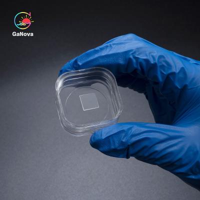
Grado electrónico solo Crystal Diamond, N Content<100ppb, conductividad termal de JDCD05-001-003 10*10mm2*0.3m m de XRD<0.015º
Precio: Negotiable
MOQ: Negotiable
El tiempo de entrega: 3-4 week days
Marca: GaNova
Destacar:Electronic Grade Single Crystal Diamond, 10*10mm2*0.3mm Single Crystal Diamond
diamante cristalino del gradiente electrónico de 10*10mm2*0.3m m solo, contenido de N<100ppb>
DescripciónLas obleas monocristal del diamante permiten avances críticos en ambos tecnología del poder del RF usada para las comunicaciones 5G y los satélites; así como en la electrónica de poder... Ver más
Contacta ahora

Procesamiento térmico rápido para aumentar la producción Sistema de recocido RTP-SA-8
Precio: Negotiable
MOQ: Negotiable
El tiempo de entrega: 3 month
Marca: Ganova
Destacar:Boost Production Rapid Thermal Processing, Rapid Thermal Processing Annealing System
1.Basic configuration of equipment system 1.1outline The Rapid Thermal Processing is a vertical semi-automatic 8-inch wafer rapid annealing furnace, which uses two layers of infrared halogen lamps as heat sources for heating. The internal quartz cavity is insulated and insulated, and the outer shell... Ver más
Contacta ahora
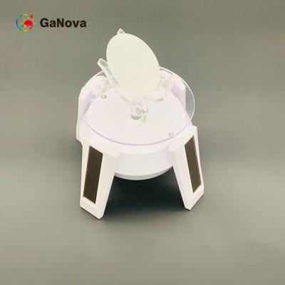
Hall Coefficient Hall Effect Sensor Tester Mobility Resistivity Measurement
Precio: Negotiable
MOQ: 1
El tiempo de entrega: 8-10week days
Marca: GaNova
Destacar:Hall Effect Sensor Tester Mobility Resistivity, carrier concentration hall effect instrument, Hall Effect Sensor Tester semiconductor
Hall Coefficient Hall Effect Sensor Tester mobility resistivity measurement Product Overview: Hall effect tester is used to measure the carrier concentration, mobility, resistivity, Hall coefficient and other important parameters, and these parameters of semiconductor materials to understand the ele... Ver más
Contacta ahora
AlN 10*10mm2 AlN cristal único 400±50μM grado S/P/R
Precio: Negotiable
MOQ: 1
El tiempo de entrega: Negotiable
Marca: GaNova
Destacar:ALN aluminum nitride wafer, 2H aluminum nitride wafer, 10*10mm2 aln wafer
AlN substrate is one of the most popular ceramic substrate which has excellent heat resistance, high mechnical strength , abrasion resistance and small dielectric loss . The surface of AlN substrate is quite smooth and low porosity . Aluminium Nitride has higher thermal conductivity , compared to al... Ver más
Contacta ahora

94um Laser Diode Chip Slope Efficiency 1.0W/A Wavelength 915nm
Precio: Negotiable
MOQ: Negotiable
El tiempo de entrega: Negotiable
Marca: GaNova
Destacar:94um Laser Diode Chip, high power laser diode chip, 1.0W/A Laser Diode Chip
94μm Laser Diode Chip Slope Efficiency 1.0W/A Wavelength 915nm 915nm 10W COS Diode Laser Chip On Submount Design For low power consumption it is essential that the output from the laser diode (LD) is efficiently coupled to the optical waveguide, and there are several approaches reported in the liter... Ver más
Contacta ahora

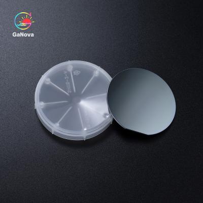
JDZJ01-001-006 Cristal de semillas de SiC de grado S de 6" Φ153±0,5 mm
Precio: Negotiable
MOQ: Negotiable
El tiempo de entrega: 3-4 week days
Destacar:Cristales de semillas de SiC de 6 pulgadas, Cristales de semillas de SiC de grado S, φ153±0, 5 mm Cristal de semillas de SiC
Sic grado 6" del cristal de semilla S grado φ153±0.5mm de S
Sic puede soportar una pendiente del voltaje (o el campo eléctrico) sobre ocho veces mayor que el Si o el GaAs sin experimentar avería de avalancha. Este campo eléctrico de la alta avería permite la fabricación de dispositivos muy de a... Ver más
Contacta ahora
Oblea Ga2O3
(13)
JDCD04-001-007 10x10mm2(010) Sustrato de cristal único Ga2O3 independiente dopado con Sn Pulido único de grado de producto
Precio: Negotiable
MOQ: Negotiable
El tiempo de entrega: 3-4 week days
Marca: GaNova
Destacar:Substrato monocristalino de Ga2O3 en pie libre, Categoría de producto Substrato de cristal único Ga2O3, 10x10mm2 Ga2O3 Substrato de cristal único
10x10 mm2(010) Sustrato monocristalino de Ga2O3 independiente dopado con Sn Pulido simple de grado de producto filtros UV
Mientras que los dispositivos basados en silicio han sido capaces de producir dispositivos relativamente eficientes, las características mejoradas del nitruro de galio dan ... Ver más
Contacta ahora
oblea de silicio
(26)
JDCD06-001-004 Wafer de silicio de 5 pulgadas Dispositivos MEMS Circuitos integrados Substratos dedicados para dispositivos discretos
Precio: Negotiable
MOQ: 1
El tiempo de entrega: 3-4 week days
Marca: GaNova
Destacar:Circuitos integrados Wafer de silicio, Discreto de los Dispositivos de Wafer de silicio, Wafer de silicio de 5 pulgadas
Dispositivos MEMS de oblea de silicio de 5 pulgadas, circuitos integrados, sustratos dedicados para dispositivos discretos
Descripción general
Aunque los cristales de silicio pueden parecer metálicos, no son del todo metales.Debido a los "electrones libres" que se mueven fácilmente entre los á... Ver más
Contacta ahora
Sapphire Wafer
(19)
C-avión Sapphire Substrate Wafer de JDCD08-001-006 6inch
Precio: Negotiable
MOQ: Negotiable
El tiempo de entrega: Negotiable
Destacar:6inch Sapphire Substrate Wafer
C-avión Sapphire Substrate Wafer de JDCD08-001-006 6inch
Los zafiros están en segundo lugar solamente a los diamantes en durabilidadEl diamante es el elemento natural más durable en la tierra y las filas como 10 de 10 en la escala de Mohs de la dureza mineral. Los zafiros son también muy durabl... Ver más
Contacta ahora

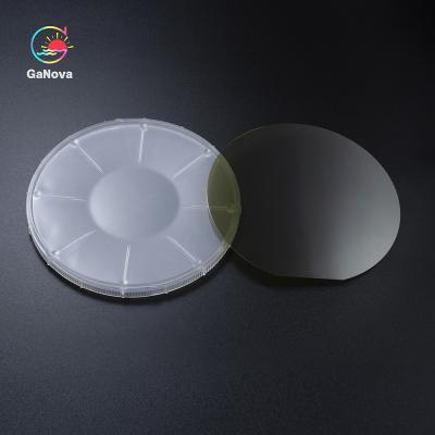
UKAS Patterned Sapphire Substrates Flat Edge Angle
Precio: Negotiable
MOQ: 1
El tiempo de entrega: Negotiable
Marca: GaNova
Destacar:UKAS Patterned Sapphire Substrates, al2o3 substrate 430um, Patterned Sapphire Substrates OEM
50.80±0.10mm Patterned Sapphire Substrates Flat Edge Angle A-Plane±0.2o 2inch Patterned Sapphire Substrates,LED Chip,Substrate Material The efficacy enhancement of GaN-based LEDs with the patterned-sapphire substrate technique is generally attributed to the improvement in both light extraction effic... Ver más
Contacta ahora

Titular de oblea de teflón de 6 pulgadas Limpieza de cestas y manijas de flores
Precio: Negotiable
MOQ: 1
El tiempo de entrega: Negotiable
Destacar:6inch Wafer Holder, wafer cassette carrier, 25 PCS Wafer Holder
6inch Wafer Holder Cleaning Flower Baskets And Handles PFA Cassette / Cassette of wafer can be customized and designed by customers’ request, able to resist strong acid, strong hydrofluoric acid, strong base and heat up to 200~220℃, use to deliver wafers in acid & base process of Fabrication f... Ver más
Contacta ahora

0.1mm/s To 600mm/s Wafer Dicing Machine X Axis Cutting Range 260mm
Precio: Negotiable
MOQ: 1
El tiempo de entrega: 8-10week days
Marca: GaNova
Destacar:0.1mm/s Wafer Dicing Machine, wafer saw machine 260mm, 600mm/s Wafer Dicing Machine
DAD3350 Wafer Dicing Machine 0.1 ~ 600mm/s X-Axis Cutting Range 260mm Improved throughput The DAD3350 achieves improvement in throughput by increasing the speed of each axis. Ease of use Operability is improved with installation of an LCD touch screen and Graphical User Interface (GUI). Easy operati... Ver más
Contacta ahora